

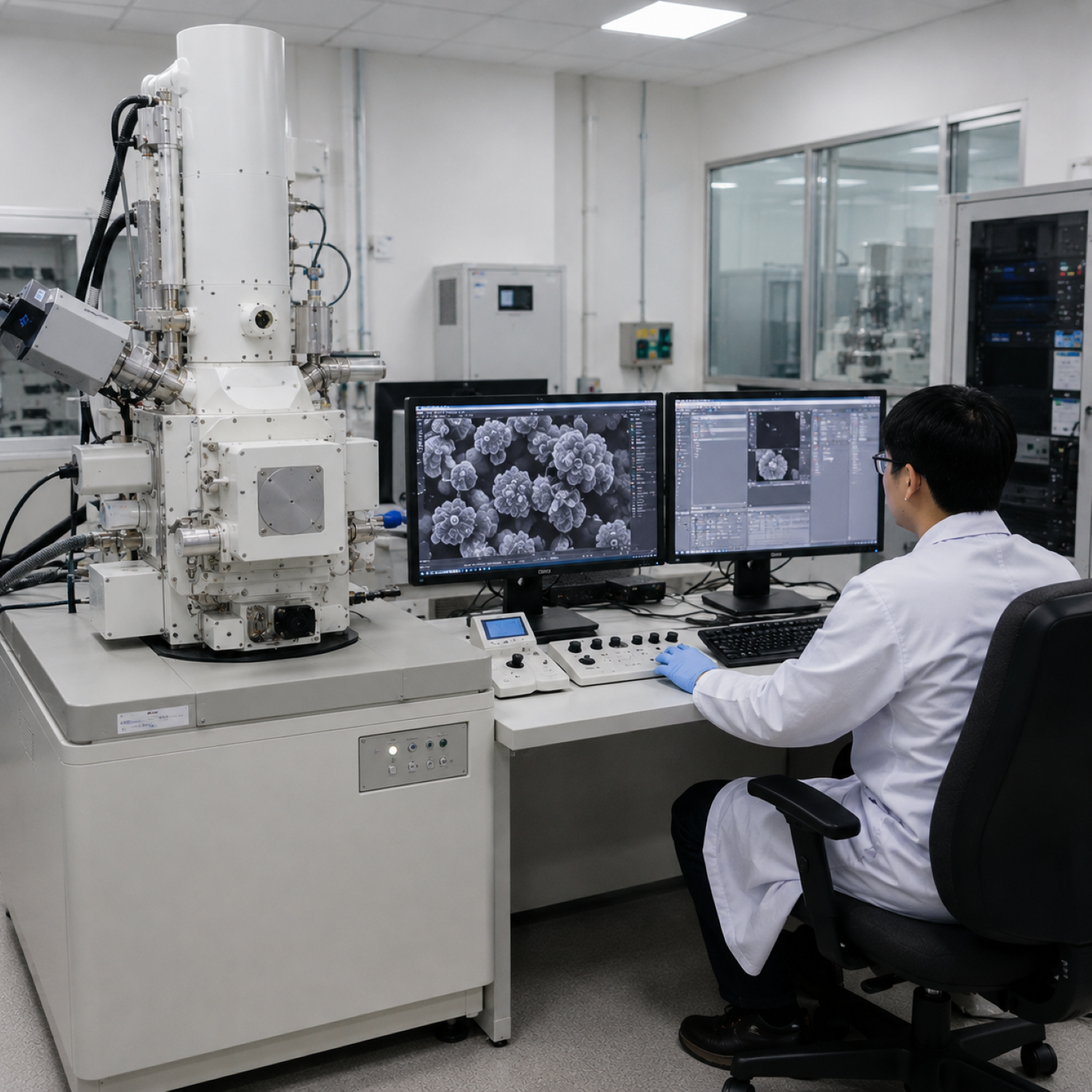
Scanning electron microscopy analysis is an important technique for understanding material defects, surface damage, contamination, and failure causes. It allows engineers and quality teams to examine a sample at much higher magnification than ordinary visual inspection or optical microscopy.
When a product cracks, corrodes, wears out, breaks, or fails unexpectedly, the visible damage is often only part of the story. SEM analysis helps reveal fine surface details that can support root cause investigation and corrective action.
How SEM Helps Identify Material Problems
A scanning electron microscope uses a focused electron beam to scan the surface of a sample. The signals generated from the sample create detailed images of surface morphology. This makes it possible to observe cracks, pits, fracture patterns, particles, corrosion products, coating defects, and other microscopic features.
When combined with EDS or EDX elemental analysis, SEM can also help identify the chemical elements present in a particle, residue, or damaged area. This is useful when investigating contamination, unknown deposits, corrosion, or material mix-ups.
Common Applications in Industry
Scanning electron microscopy analysis is used across automotive, electronics, aerospace, metal processing, plastics, coating, and precision manufacturing. It can support failure analysis, material characterization, contamination analysis, and quality control.
For automotive components, SEM can be used to examine fracture surfaces, coating adhesion issues, wear particles, corrosion marks, or foreign particles found during cleanliness testing. For electronics, it can help inspect solder joints, conductive residues, cracks, and surface defects.
Why SEM Is Useful for Failure Analysis
Failure analysis often requires more than one test method. SEM provides high-resolution images that help explain how damage started and how it developed. For example, a brittle fracture, fatigue crack, ductile overload, corrosion attack, or wear-related failure may leave different surface features.
By studying these patterns, technical teams can narrow down whether the problem may relate to material selection, processing conditions, design stress, contamination, heat treatment, or service environment.
Turning Microscopic Evidence into Corrective Action
The goal of scanning electron microscopy analysis is not only to produce detailed images. The real value is in connecting those images with production history, material data, and product performance.
When SEM results are interpreted properly, manufacturers can make better decisions about supplier control, process adjustment, material improvement, cleaning validation, or product redesign. This makes SEM a practical tool for reducing repeated failures and improving product reliability.